Fabricating PCBs with the Toner-Transfer Hobby-Knife Method
August 22, 2013 4 Comments
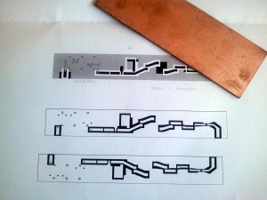 I needed to prototype a UHF front-end for the USRP. I did not want to use a PCB fabrication service, both because I forgot how to use Eagle and because I wanted the PCB as quickly as possible.
In the past I constructed circuits on copper-clad boards by cutting isolation channels between pads with a hobby knife. This works well for simple circuits, especially when combined with the “dead-bug” technique (as I’ve done here, for example). Dead-bug did not seem like appropriate technique for UHF, but the circuit I wanted to build was certainly very simple, so creating all the traces and pads by cutting isolation channels seemed plausible.
However, most of the components in this circuit are surface-mount components, and some are pretty small. The most challenging part was a 3mm-by-3mm SAW filter. The pads for it on the PCB need to be separated by about 0.5mm (the manufacturer recommends a separation of 0.38mm). This required precision; I needed to know exactly where to cut. In the past I cut the isolation channels free hand, but this job called for precision.
I decided to try to use the toner-transfer technique to transfer a PCB design from the computer to paper to the copper-clad board. Once the design was “printed” on the copper, I would cut out the channels with a hobby knife.
I started by drawing the design in Adobe Illustrator. I copied the footprints from the data sheets to Illustrator, then combined them into a circuit and drew the connecting traces and the ground plane. I printed out the design and checked that the components actually fit their pads. I then copied the design in illustrator and transformed the drawing until the copper was in white and the isolation channeled (“etched” areas) were in black. Finally, I created a mirrored version and printed it out. You can see all three phases in the picture above, along with the two-sided copper-clad board I used later.
Note that this printout is the reverse of what you need to etch using the toner-transfer method. When you etch (I used to do it years ago but now I don’t want to deal with the chemicals) using toner transfer you print in black the areas where the copper should remain.
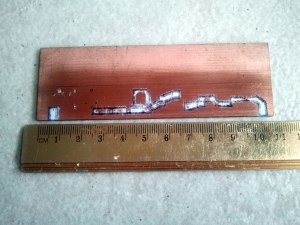 I printed the design on a laser printer on plain paper, even though glossy is supposed to work better. I taped the paper to the copper-clad board and ironed it for a few minutes. This leaves the paper glued to the copper (the toner is the glue), so I soaked the paper and carefully removed most of it. You can see the result on the right. I did not bother to remove all the paper, and I did not worry about partial transfers, because I was not going to etch the board, just to use the black toner as a marker for where to cut and drill. Some parts did not transfer well, mostly very thin lines. But most of it trasfterred well, including the sub-millimeter lines around the SAW filter.
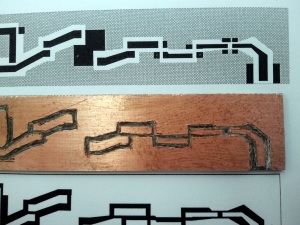 Now it was time to remove the copper from the isolation channels. I cut along the edges of the black lines with a hobby knife. The knife feels different when it is cutting through the soft copper than when it cuts through the fiberglass board, so you know when you cut through the copper. I worked by trying to cut V-shaped channels in the board. Initially I tried to use a ruler to get straight lines, but after a while I realized that it would be easier to cut free hand. The lines might not be perfectly straight, but not to an extent that matters. You can see the result in the picture. I think it looks pretty close to the design. Don’t be misled by the picture; the channels are really narrow, around 0.5mm at the narrowest, and the narrow traces are about 1mm or a bit less.
![]() After drilling holes for one through-hole component, for vias to two traces on the other side, and for some vias to connect the ground plane on both sides, the board was ready for soldering.
After drilling holes for one through-hole component, for vias to two traces on the other side, and for some vias to connect the ground plane on both sides, the board was ready for soldering.
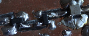 As expected, soldering the 3mm SAW filter was challenging, but it worked. The other components were easy to solder, even the 0603 capacitors and the SOT-89 amplifier. When I designed the board, I left quite a lot of space between components (around 4mm) to make soldering easy. It was easy, but I think it would have been easy even if the components were packed much tighter. A lesson for the future.
The finished board looks okay and from limited testing I’ve done so far, it works correctly. It certainly amplifies and filters.
The whole process took a few hours. It’s not a super-quick method, but not too consuming either. No chemicals and no waiting for commercially-made PCBs. I’m pretty happy with the result.
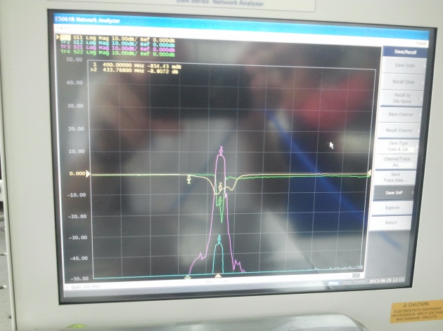
An update from August 29: After putting the unit in a metal box, I measured its performance with a network analyzer (thanks to Avigdor Drucker for helping out). It performed very well, with good gain and excellent filtering, as you can see in the screen shot below. At least at these UHF frequencies, this technique can deliver good results.

Hi Sivan,
There is a knife that is better to cut thin V-shaped channels. It is called a Formica knife. Ask about it in any good tools shop.
Victor – 4Z4ME
Thanks a lot Victor. I’ll give it a try. Sivan
Pingback: Rebuilding a Heathkit HP-23 Power Supply | Eclectic Technical Experiences
Pingback: A Selective and Robust UHF Front-End | Eclectic Technical Experiences