Surface-Mount (SMD) Prototyping and Hacking
July 7, 2017 Leave a comment
A huge range of electronic devices now come only in surface-mount (SMD) packages, so techniques for prototyping with these devices are often useful. Also, most ready-made boards use these devices, so if you need to modify such a board, similar techniques are helpful.

The picture above shows such a prototype. I built the circuit on a piece of SMD prototyping board made by BusBoard. The squares are 50mil (0.05 inch) by 50mil. The small square device at the top is a 1.2mm by 1.2mm Hall-Effect sensor; its 4 contacts are spaced 0.65mm apart. The larger device next to it is a MOSFET in an SC59 package. The brown capacitor next to it and the two black resistors are in 0603 packages. It’s a simple circuit. It was not hard to prototype like this, and testing it gave me very useful insights and a lot of confidence before designing a PCB and ordering a batch of assembled units to test.
Obviously, some SMD packages are easier to prototype with than others. The same MOSFET (a DMN1019) also comes in a smaller 1.95-by-1.95mm package, so in the PCB design intended for automated assembly, I used the smaller package to save space. I bought the SC59 device simply to make prototyping easier.
The picture below shows another example of the same technique on the same type of prototyping board. This circuit is a 1.8V regulator, and here too the capacitors are 0603.
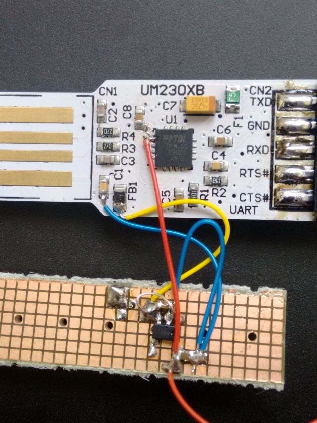
The picture also shows how I hacked a ready-made board, a USB-to-UART bridge with an FTDI FT230X chip. The chip can support a variety of I/O voltages, but the board is wired for 3.3V and there is no easy way to change this. I needed the UART to work at 1.8V, so I added the regulator on the BusBoard. But I also needed to cut a trace between the 3.3V supply on the ready-made board and a pin of the FT230X, and to connect to that pin the 1.8V supply. The red wire carries this supply voltage to the pin.
The thin hookup wires I use are old wire-wrap wires. They are often convenient. To connect to the pin of the QFN chip the thin wire was certainly helpful.
These techniques are useful for simple circuits (or in these case, for small parts of circuits that are attached so a hacked board), but it is hard to scale this up to more complex circuits. For complex circuits, it is better to design a PCB and have it manufactured, even for a prototype. A PCB makes it possible to use a much wider variety of packages than is possible with the BusBoard boards, and the solder mask makes solder bridges much less likely; the lack of solder mask is one of the disadvantages of the BusBoard technique.
To end, here is another example of SMD prototyping, here an SPI NAND flash chip, placed upside down on a conventional 0.1″ prototyping board. It’s ready to be hooked up to a microcontroller for testing. It’s 8 pads are spaced about 1mm apart.

